
ChipStart ASIC Design
World-Class Semiconductor IP Without Starting from Scratch.
Designing a custom ASIC or integrating semiconductor IP shouldn't mean months of ramp-up, hand-rolled infrastructure, and reinventing the wheel. ChipStart® ASIC Design gives semiconductor, consumer electronics, and IoT companies access to proven analog and digital IP blocks, expert integration services, and a deep partner ecosystem so you can move faster, reduce risk, and put your engineering resources where they matter most.
Custom Silicon Is Hard.
The Right IP Partner Makes It Manageable.
Every ASIC design project starts with a familiar tension: the pressure to ship on time, the complexity of integrating reliable IP, and the risk of choosing the wrong building blocks at the wrong stage of development.
Building analog and digital IP in-house is expensive, time-consuming, and often extraneous to your core differentiation. Sourcing from fragmented vendors adds integration risk and support uncertainty. And navigating the ASIC ecosystem, from design and testing tools to foundry relationships to EDA partnerships, requires experience most lean engineering teams don't have the bandwidth to develop.
ChipStart was built for exactly this problem. We bring proven IP, deep integration expertise, and a trusted partner network to your design program so your team can focus on the innovation that actually wins in the market.
The ChipStart Advantage
Choosing the right semiconductor IP and integration partner isn't just a technical decision. It's a business decision that shapes your schedule, risk profile, and competitive position. ChipStart is built around four principles that translate directly into better outcomes for your design program.
It starts with performance you can rely on and extends to the ability to embed the latest functional advances without having to start over. We deliver the economics that keep your program viable with IP that's structured to protect and amplify your investment.

Performance Efficiency – Our analog and digital IP blocks are engineered for efficiency and validated across process nodes and design environments. They deliver the timing, area, and power characteristics your architecture requires, optimized for your configurations, rather than inherited from other designs' constraints.

Functional Advancements – The semiconductor landscape evolves rapidly with new processes, technologies, and interface standards. Our portfolio of current-generation IP is designed to adapt to your product roadmap evolution, keeping pace with functional demands while eliminating expensive re-architecture every product cycle.

Cost Optimization – Building IP from scratch is expensive and time-consuming. Fragmented IP from multiple vendors increases integration costs and support risk. We consolidate proven IP, expertise, and ecosystem partnerships into one engagement that optimizes cost, compresses schedules, and delivers faster tapeouts with fewer surprises.

Design & IP Selection – Architecture-stage decisions determine design economics. We bring integration expertise and deep IP portfolio to early-program stages, helping your team make smart build/buy/license trade-offs before they're costly to change. We optimize existing IP portfolios for maximum reuse and minimal redundancy.
Together, these advantages mean you're not just getting an IP design partner. You're tapping into a wealth of knowledge and experience that can help you optimize your operations and resources to deliver a better product that drives business growth.


Trusted Partner Network
Great ASIC design doesn't happen in a vacuum. It depends on the right EDA tools, the right foundry relationships, and partners who have worked together long enough to know where the integration bodies are buried.
ChipStart has spent years building and maintaining relationships across the semiconductor design ecosystem, from EDA vendors and IP libraries to foundry partners and reference design programs.
When you work with ChipStart, you inherit that network.
Design Tool Ecosystem – Our IP and integration services are validated against industry-standard EDA platforms, ensuring that the IP you license or integrate doesn't create toolchain friction in your existing design environment.
Foundry & Process Relationships – Our team has direct experience working across leading process nodes and foundry environments to reduce the risk of process-level surprises late in the design cycle.
Industry Partner Program – We maintain active relationships with complementary IP vendors, design services firms, and semiconductor industry organizations, giving clients access to an expanded ecosystem to support a robust design program.

Semiconductor IP and Integration Services
ChipStart ASIC Design empowers clients to accelerate innovation and efficiency. Our services are integral to a wide range of consumer and industrial technologies, delivered across the following core service capabilities:
Semiconductor IP Design
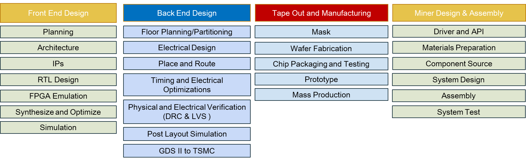
Custom ASIC design for semiconductor chips, covering FPGA, ASIC, and related design work from initial architecture all the way through tape-out and final production.
IP Integration
End-to-end IP integration consulting and delivery, from architecture review through tape-out support. ChipStart works alongside your engineering team to manage the complexity of integrating third-party and proprietary IP blocks.
IP Aggregation & Licensing
IP portfolio aggregation and licensing program management for companies looking to structure and commercialize their IP assets.
Packaging Services
SoC System Management Service (SSM)
Centralized system management architecture for complex SoCs that provides integrated hardware IP and software for power management, security, boot control, error handling, system monitoring, and platform management functions.
Custom Memory Design
Memory configuration, selection, integration, and performance tuning to optimize bandwidth, latency, power consumption, and overall system efficiency.
Product Engineering
ChipStart delivers turnkey product engineering solutions from initial prototyping through mass production, backed by a fully integrated supply chain. Our advanced technology design helps customers build their business efficiently, expediting time-to-market and time-to-volume. For Digital Currency, we manage the full lifecycle for our customers. This starts with chip design and chip manufacturing to system design and system manufacturing, spanning hardware, software and cloud services.
Let's Talk About Your Design Program
Whether you're sourcing IP, evaluating integration support, or building out a licensing program – we'd like to hear about what you're working on.